
Design process of 3D metamaterial using spatial transforms

Introduction
Electromagnetic fields cannot be controlled inside a real, homogeneous material. However, these fields can be controlled by changing a local value of effective permeability and/or permittivity. It's may be done by use a some periodic structures (unit cell). Transformation optics (TO) [5–7] is one technique for designing periodic structures that are macroscopically inhomogeneous. The TO technique takes a spatial transform as the input, applies it to Maxwell's equations, pulls the transform out of the spatial coordinates and incorporates it into the constitutive parameters. Next step is generating the geometry of spatially variant lattices. This is a big challenging because the electromagnetic properties of the lattice depend on the size, direction and shape of the unit cells. Also often require adjacent unit cells to be the same, and shapes changing should be continuous, without distortion. This structure may be made (printed) by 3D printer.
- Methods
Design process of 3D metamaterial using spatial transforms is presented in a four-step:
- 1. The first step is to define a how the fields or waves should be bent or directed in space
- 2. The second moves the spatial description of wave behavior into the spatial parameters μ and ε. In other words, in this step, produces a map of the permeability and permittivity as a function of position. To make this transformation a optical transformation may be used.
- 3. In this step converts the maps of μ and ε into maps of geometrical parameters that are to be spatially varied throughout the material.
- 4. Last step is to generate the overall spatially variant lattice that is smooth, continuous, free of defects and that correctly realizes the required geometry at every location in the lattice.
- Results
Using Fourier Expansion method (see Fig 1 and 2) we designed a lens for microwave band (around 10 GHz - 12 GHz). Unit cell was taken from [4]. Size of unit cells are constant and is associated with the wavelength. The lens has been designed by modulating the fill factor (FF) of each cell (from 0.25 to 0.65, see fig. 2). Fig 3 present a field distribution around our lens in full EM simulation. The source wave is plane wave. The lens was printed on a 3D printer and its physical parameters were measured (Fig 4).
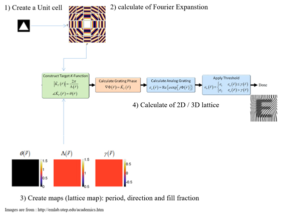
Fig 1: Fourier Expansion method
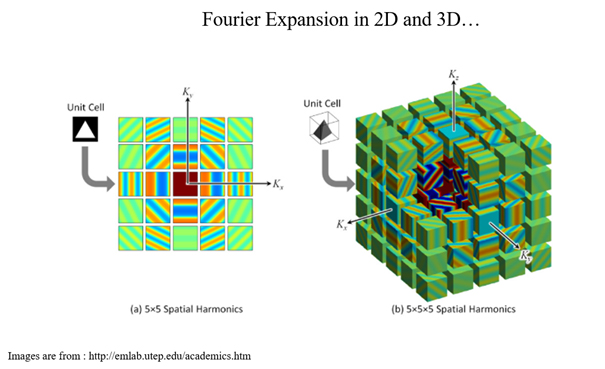
Fig 2: Fourier Expansion method in 2D and 3D
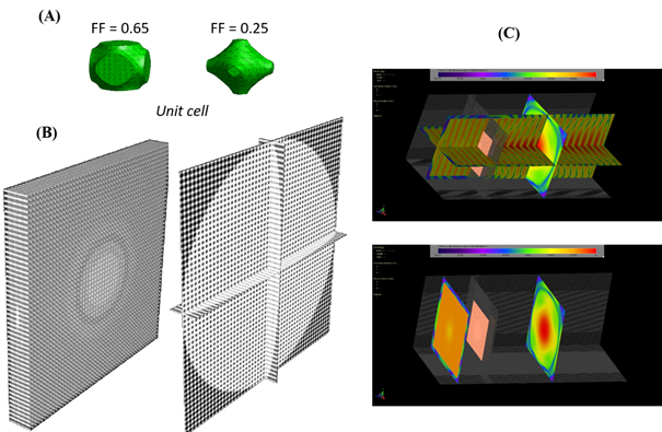
Fig 3: 3D metamaterial lens made from dielectric: (A) unit cell with different fill factors, (B) 3D structure of lens, (C) Electomagnetic field distribution around lens obtain from full electromagnetic simulation.
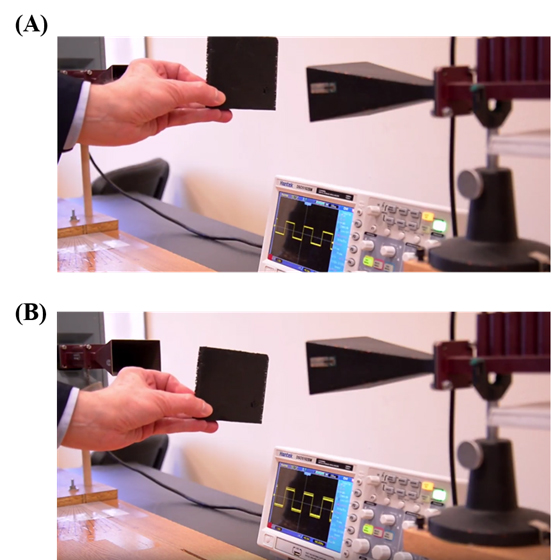
Fig 4: 3D printer lens in microwave track: (A) lens out of track, (B) lens placed in the track.
- Conclusions
- Contact
- Dr. Łukasz Jopek
 , e-mail: This email address is being protected from spambots. You need JavaScript enabled to view it.
- Dr. Łukasz Jopek
- Publication
- Chen H, Chan C& Sheng P. 2010Transformation optics and metamaterials. Nat. Mater. 9, 387–396.
- Kwon D-H& Werner DH. 2010Transformation electromagnetics: an overview of the theory and applications. Antennas Propag. Mag. IEEE 52, 24–46.
- Pendry JB, Schurig D& Smith DR. 2006Controlling electromagnetic fields. Science 312, 1780–1782.
- Rumpf Raymond C., Pazos Javier J., Digaum Jennefir L. and Kuebler Stephen M. 2015, "Spatially variant periodic structures in electromagnetics" Phil. Trans. R. Soc. A.37320140359