Design process of 3D metamaterial using spatial transforms
Design process of 3D metamaterial using spatial transforms

Introduction

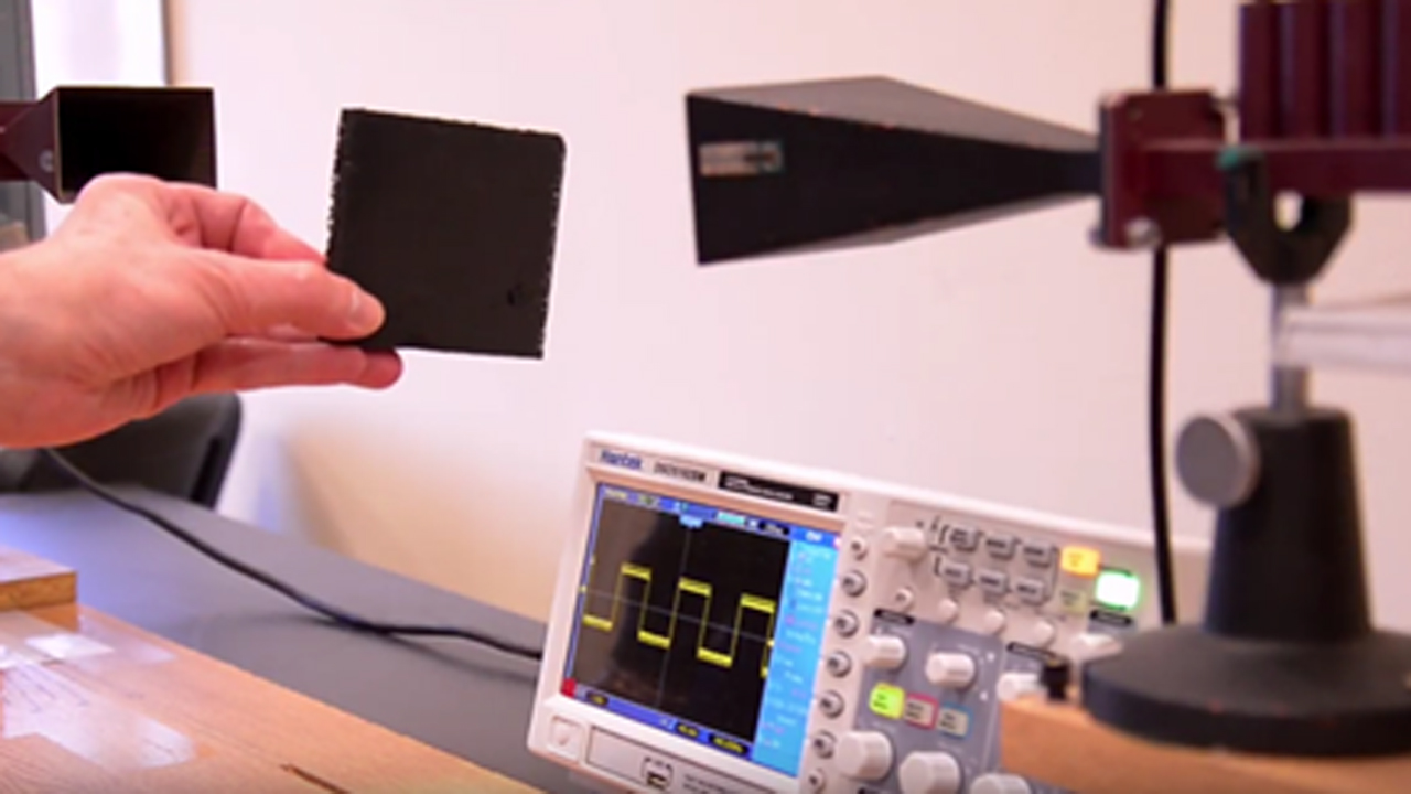
Electromagnetic fields cannot be controlled inside a real, homogeneous material. However, these fields can be controlled by changing a local value of effective permeability and/or permittivity. It's may be done by use a some periodic structures (unit cell). Transformation optics (TO) [5–7] is one technique for designing periodic structures that are macroscopically inhomogeneous. The TO technique takes a spatial transform as the input, applies it to Maxwell's equations, pulls the transform out of the spatial coordinates and incorporates it into the constitutive parameters. Next step is generating the geometry of spatially variant lattices. This is a big challenging because the electromagnetic properties of the lattice depend on the size, direction and shape of the unit cells. Also often require adjacent unit cells to be the same, and shapes changing should be continuous, without distortion. This structure may be made (printed) by 3D printer.

Continue Reading

Artificial Magnetic Conductor (AMC)

Artificial Magnetic Conductor

Introduction

Artificial Magnetic Conductor (AMC) structures [1, 2] also known as High Impedance Surface (HIS). One of most interesting application of AMC is in the design of efficient and low-profile antennas [3–7]. Currently known AMCs are inherently frequency-selective and suffer from narrow band property which limits their applications in wideband or multiband antenna applications. The particular area of interest in this study is the investigation into the possibility of employing automatic optimization of elementary AMC cell geometry to tune its frequency characteristics i. e. its center frequency and bandwidth.

Continue Reading

Modeling Field Circuit

Modeling Field Circuit

Introduction

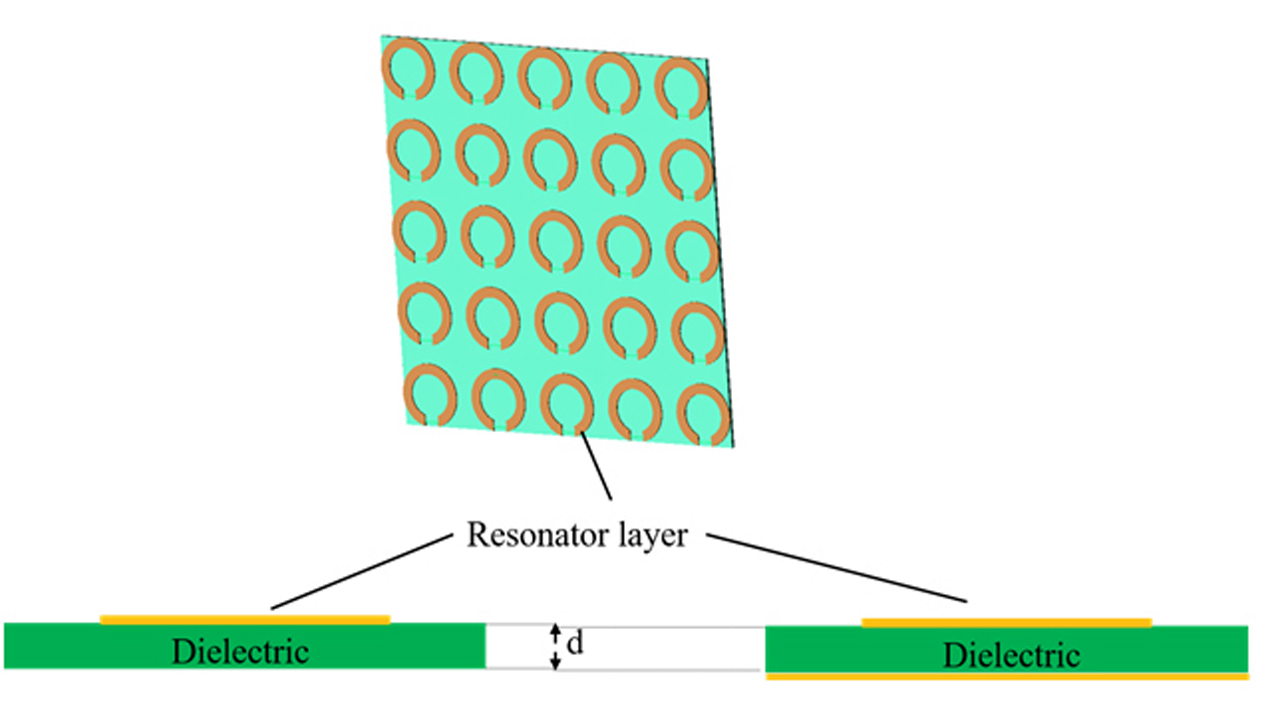
Metamaterials have become a very active research area because of the possibility of creating materials which exhibit unusual EM responses not attainable with natural materials. Some application examples are in superlensing, cloaking, artificial magnetic conductance and more generally, coordinate transformation material design [1]. To realize such functionalities, periodic or semi-periodic arrays of resonant structures such as split-ring resonators (SRRs) have been successfully used [2]. Metasurfaces can be successfully analyzed using full electromagnetic simulation. Unfortunately, however numerical simulations are methods of high computational complexity, and need a long time to computing.

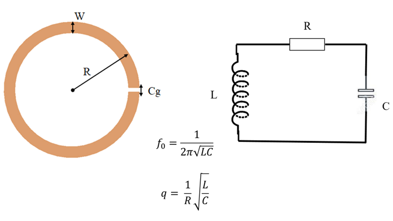
On the other hand, a single SRR can be regarded as a resonant circuit with an inductance (following from the ring geometry only), a capacitance (following from the split in the ring and from the whole conducting surface) and a resistance of the conductor. Typically, dimensions of the structure are small compared to the resonant wavelength which helps to achieve low radiative losses and high quality factor (Q-factor).

Circuit-based model of SRR is a low-computational, very fast method to behavior simulation of single SRR. If, we combine this with model of impacts between SRRs then we can modeling of SRR network.

Continue Reading

Institute Structure – Divisions

Medical Electronics Division

Head of the Division
prof. Piotr Szczypiński


Communications Division

Head of the Division
prof. Sławomir Hausman


Electronic Circuits and Thermography Division

Head of the Division
prof. Bogusław Więcek

Address

Institute of Electronics
Lodz University of Technology
Al. Politechniki 10, B-9 building
93-590 Lodz, POLAND


Correspondence address

116 Żeromskiego Str.
PL 90-924 Lodz
POLAND

VAT identification number: PL 727-002-18-95