
Modeling Field Circuit

Introduction
Metamaterials have become a very active research area because of the possibility of creating materials which exhibit unusual EM responses not attainable with natural materials. Some application examples are in superlensing, cloaking, artificial magnetic conductance and more generally, coordinate transformation material design [1]. To realize such functionalities, periodic or semi-periodic arrays of resonant structures such as split-ring resonators (SRRs) have been successfully used [2]. Metasurfaces can be successfully analyzed using full electromagnetic simulation. Unfortunately, however numerical simulations are methods of high computational complexity, and need a long time to computing.
On the other hand, a single SRR can be regarded as a resonant circuit with an inductance (following from the ring geometry only), a capacitance (following from the split in the ring and from the whole conducting surface) and a resistance of the conductor. Typically, dimensions of the structure are small compared to the resonant wavelength which helps to achieve low radiative losses and high quality factor (Q-factor).
Circuit-based model of SRR is a low-computational, very fast method to behavior simulation of single SRR. If, we combine this with model of impacts between SRRs then we can modeling of SRR network.
- Methods
1. Resonator model
Our analytical model is based on the equivalent circuit description of coupled resonators with closed-form expressions for the surface charge and current densities along a circular SRR. Our coupled SRRs are analyzed using their equivalent LCR circuit. Single SRR may be description as a series RLC circuit, where all physical quantities are described using lumped elements - see Fig 1a. For example Inductance is represented by ideal coil, capacity of gap by ideal capacitor etc.
Small loop theory assumes uniform current around the loop. Where loop shape is less than around 10% wavelength, current is nearly constant, within a few percent. As frequency increases, and the loop size is more like 20-30% wavelength, current is not uniform and can vary as much as several dozen %. Because of that the distributed model should be considered. In opposite to previous one, resonator forming conductor is divided into (very) small segments - see Fig2.
2. Mutual coupling model
The mutual inductance coupling between any two coils (Fig. 1.) can be related to their self-inductance by means of the coupling constant km (1) and self-capacitance (2) which can take on positive or negative values.
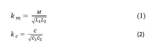
where M denotes magnetic mutual coupling between coils [4], C denotes electric mutual coupling, L1, L2 represent the self-inductance of coils, C1, C2 represent the self-capacitances of resonator. On the other hand km factor may be defined considering the ratio of coupled energy to stored energy (2) [5].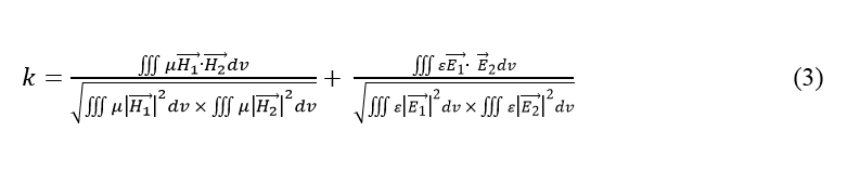
where H represent the magnetic field vectors and E represent the electric field vectors.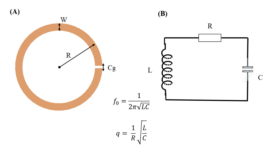
Fig. 1: Equivalent circuit based model of single Split ring Resonator (lumped-element model)
![Fig. 2: Equivalent circuit based model of double Split ring Resonator (distributed-element model) [4,5].](/eng/images/joomlaplates/research/sc_telecom/sc_circuit_05.jpg)
Fig. 2: Equivalent circuit based model of double Split ring Resonator (distributed-element model) [4,5].
- Results
To efficiently design metasurfaces for a given application a hierarchical (Particle Swarm Optimization and Evolutionary Optimization) will be used (see Figure 1). The first level of the algorithm uses the Particle Swarm Optimization (PSO). PSO needs a high number of objective function computations (approximately the number of particles multiplied by the number of algorithm iterations). Therefore fast computation of the direct-problem and the objective function is needed (circuit-based equivalent model). On next level a more time consuming objective function can be used (EM simulation). The evolutionary algorithm typically requires fewer calls to the objective function. General scheme is show on fig 3.
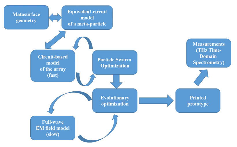
Fig.3: General scheme for metasurface modeling with circuit and field based models.
- Conclusions
- Contact
- Dr. Łukasz Jopek
 , e-mail: This email address is being protected from spambots. You need JavaScript enabled to view it.
- Dr. Łukasz Jopek
- Publication
- [1] Tong, X. C., “Functional Metamaterials and Metadevices, Springer Series in Materials Science”, Springer, 2018.
- [2] R. A. Shelby, D. R. Smith, and S. Schultz, “Experimental verification of a negative index of refraction,”, Science 292, 77–79 (2001).
- [3] S. Babic, F. Sirois, C. Akyel and C. Girardi, “Mutual Inductance Calculation Between Circular Filaments Arbitrarily Positioned in Space: Alternative to Grover's Formula”. in IEEE Transactions on Magnetics, vol. 46, no. 9, pp. 3591-3600, Sept. 2010.
- [4] Solymar L., and Shamonina E.:. 2009. Waves in Metamaterials. Oxford University Press, Inc., USA.
- [5] Shamonin M ., Shamonina E., Kalinin V., Solymar L.: ” Properties of a metamaterial element: Analytical solutions and numerical simulations for a singly split double ring”, Journal of Applied Physics 2004 95(7):3778